“极端光学研究创新团队”胡小永教授和龚旗煌院士在微纳全光交换器件的研究中取得新进展。芯片上全光交换能够将任意一个输入波导中的信号光切换到任意一个输出波导,是实现超高速超宽带信息处理芯片和光计算的最核心器件之一,其实用化要求的重要指标是:超低能耗、超快响应、片上触发、多波长(或宽带)操作。实现机理是利用三阶非线性光学Kerr效应,即信号光(或控制光)诱导折射率改变。一方面,由于通常的半导体材料和有机聚合物材料的三阶非线性光学系数相对较小,单纯依靠硅基光子学和有机光子学很难实现片上低能耗超快全光交换;另一方面,由于贵金属材料内在的欧姆损耗导致表面等离激元较大的传输损耗,单纯利用表面等离激元很难实现大规模片上超快光交换阵列。因此,目前国际上在该领域的实验研究中存在的难题是,难以在集成光子回路中实现超低能耗、超快响应、片上触发、多波长操作的全光交换。
研究论文提出一种复合增强三阶非线性新方法、以及表面等离激元-介电光子纳米复合结构新构型,获得了同时具有皮秒量级超快响应和巨大三阶非线性系数的多组分纳米复合材料nano-Au:(IR140:PDTP-DFBT),并且将表面等离激元和介电光子学的优势相结合,以具有强光场局域和场增强效应的表面等离激元纳米复合腔作为开关单元,表面等离激元纳米复合腔提供片上表面等离激元感应透明,能提供4个工作波长;以超低损耗氮化硅狭缝光波导作为连接波导,制备出由氮化硅狭缝光波导连接4个表面等离激元纳米复合腔阵列所构成的片上2×2全光交换器件,利用上层控制波导的倏逝场触发开关单元来实现片上触发的全光交换的功能。将全光交换的控制光阈值光功率降低4个数量级,控制光强降低到450 kW/cm2,同时保持63 ps的超快时间响应。这样实现了超低能耗、超快响应、片上触发、多波长操作的全光交换器件。
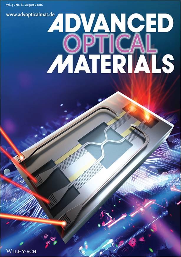
研究论文于2016年8月21日发表在重要期刊Advanced Optical Materials上(Zhen Chai, Yu Zhu, Xiaoyong Hu, Xiaoyu Yang, Zibo Gong, Feifan Wang, Hong Yang, Qihuang Gong, “On-chip optical switch based on plasmon-photon hybrid nanostructure-coated multicomponent nanocomposite”, Advanced Optical Materials Vol.4, No. 8, 1159-1166 (2016)),并被选为同期的封面文章。博士生柴真为论文第一作者。Advanced Optical Materials期刊同期评述这项工作“为克服实现超大规模集成光子回路和芯片面临的内在材料限制开辟了一条道路,还为非线性光学和量子光学的基础研究提供了一个芯片上实验室平台”。该研究工作还被WILEY出版集团科技网站Materials Views China以“表面等离激元与光子学融合:芯片上超快全光交换新突破”为题进行了专题评述。
研究工作得到国家973项目、介观物理国家重点实验室、“2011计划”量子物质科学协同创新中心、极端光学协同创新中心等的资助。
On-chip low-power micro/nanoscale All-Optical Switch
On-chip all-optical switch, possessing the unique ability of switching signal light propagating in any incident waveguide channel into any required output waveguide channel, is one of the core components of all-optical networks, and ultrahigh-speed and ultrawide-band information processing chips. For practical chip-integration applications, several significant indexes, i.e. on-chip trigger, ultrafast response, ultralow energy consumption, high switching efficiency between different waveguide channels, and wideband (or multiple-wavelength) operation, are stringently required. The basic realization mechanism of all-optical switching is based on the third-order nonlinear optical Kerr effect, i.e. the control-light induced refractive index changes. owing to relatively small third-order optical nonlinearity of conventional semiconductors and organic polymers, it is very difficult to realize a large-scale integration of on-chip-triggered all-optical switch only appealing to traditional silicon photonics or organic photonics alone. On the other hand, owing to serious ohmic losses of metal and accordingly severe propagation losses of surface plasmon polaritons (SPPs) in the near-infrared range, it is infeasible to construct a large-scale integrated plasmonic waveguide channel arrays for the all-optical switch application.
Gong’s group proposed a new compound enhancement of nonlinearity method, and a novel plasmonic-photonic hybrid nanostructure by combining the advantages of plasmonics and photonics. They obtained a multicomponent nanocomposite material nano-Au:(IR140:PDTP-DFBT) having very large third-order nonlinear optical susceptibility and ultrafast response of several picoseconds order simultaneously. On-chip plasmoni-induced transparency was achieved in the plasmonic-photonic hybrid nanocavity, which provides four operating wavelengths for the all-optical switch. Low-loss SiN slot waveguides were used as access waveguides to construct a chip-integrated 2×2all-optical switch device, switching units of which was triggered by control waveguides in the upper layer in the term of evanescent field. The control light threshold power of the all-optical switch was reduced by four orders, the control light intensity reduced to 450 kW/cm2,and an ultrafast response time of 63 ps was maintained. Therefore, an ultrafast, ultralow-power, on-chip-triggered all-optical switch with multiple operating wavelengths was realized in integrated photonic circuits directly. This work was published in Advanced Optical Materials(Zhen Chai, Yu Zhu, Xiaoyong Hu, Xiaoyu Yang, Zibo Gong, Feifan Wang, Hong Yang, Qihuang Gong, “On-chip optical switch based on plasmon-photon hybrid nanostructure-coated multicomponent nanocomposite”, Advanced Optical Materials Vol.4, No. 8, 1159-1166 (2016)),and was selected as the cover article of the journal.
This work was highly evaluated by the journal of Advanced Optical Materials: “This paves a way to overcome the intrinsic material limitations for the realization of very-large-scale integrated photonic circuits and chips, and additionally provides a lab-on-chip platform for fundamental research of nonlinear optics and quantum optics”. This work was also highly evaluated by the Materials Views China of WILEY publishing group.
The work was supported by the National Basic Research Program of China, State Key Laboratory for Mesoscopic Physics, Collaborative Innovation Center of Quantum Matter, and Collaborative Innovation Center of Extreme Optics.